Can Semiconductors Operate Like a Human Cell?
3 Aug, 2007 10:59 am
Semiconductor membranes made of two thin layers of opposite n- and p-doping can perform electrically tunable ion current rectification and filtering in a nanopore, which are fundamental functions of biological membranes surrounding human cells.
Advances in semiconductor nanotechnology has made possible the fabrication of nano-scale semiconductor layers that can be doped with either donor or acceptor impurities, thereby changing drastically the materials electrical conductivity as sustained either by negative charge carriers (electrons; n-type materials) or positive charge carriers (holes; p-type materials). The most basic solid-state devices are p-n junctions made of semiconductors of two adjacent p- and n- regions, which under external voltage bias exhibit the remarkable property of current rectifying i.e. the current only flows along one direction (forward bias), while it is blocked in the opposite direction (reverse bias).
Recent study by researchers at the University of Illinois at Urbana-Champaign shows that very thin p- and n-semiconductor materials in which a pore of a few nanometer diameter, has been created by very bright electron beam lithography can be used to produce similar functions but with higher performances than biological lipid bi-layer (1, 2).
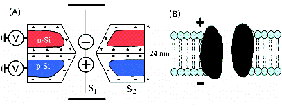
The nanopore-membrane structure geometry is shown schematically in figure 1, and consists of two 12 nm silicon (Si) layers of different doping: the top layer is n-doped with a donor concentration Nd=2X10²⁰/cm3 and the bottom layer is p-doped with an acceptor concentration Na=2X10²⁰/cm3. The nanopore in this solid-state membrane has a double-conical shape with a 1 nm diameter in the narrowest region and 6 nm diameter opening on each side of the pore as a result of the electron beam fabrication. The whole surface of the nanopore-membrane is covered by a 8 Angstroms surface layer of silicon dioxide (SiO2) containing a fixed negative charge of 2.5X10⁻⁶C/cm2. The semiconductor membrane is immersed in an electrolyte solution containing potassium chloride (KCl), with a concentration varying from 0.01M to 1 M.

Fig.1: A) Schematics of a nanopore in a p-n semiconductor membrane. Colors show the different n-(red) and p-(blue) layers with their charges as well as the induced ionic charges in the channel. B) Schematic of biological channel in a polarized lipid bi-layer. The dark area represents the protein forming the channel.
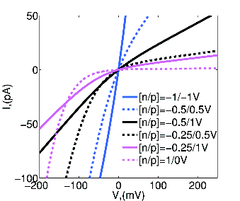
By using advanced computer modeling, the researchers at the University of Illinois have shown that the p-n membrane offers higher functionality than biological membranes or other solid state membranes made of dielectric materials. Hence, they predicted that for appropriate biasing of the membrane-electrolyte system, the ionic current (made of the two kind of ions K+ and Cl- moving in opposite directions) flowing through the nanopore can be controlled to such extend that it can exhibit either ohmic behavior as in a conventional electric resistance, or sharp rectification as in p-n junction diodes (fig.2). The presence of opposite charges in the n- and p- layers of the membrane, each controlled by independent voltage sources modifies the profile of the electric potential in the nanopore, which influences the ionic conductivity. In addition to its rectifying property, the p-n membrane is capable to operate as an ion filter whereby the nanopore could block either one of the ion current components i.e. either K+ or Cl- current, and enhance the other one. The real advantage of the p-n membrane compared to other membranes is its electrical tunability, whereby these different behaviors can be controlled by appropriate biasing of the n- and p- layers.

Fig.2: Ionic current-voltage characteristics through the nanopore of a p-n membrane for different bias between the n- and p-layers, illustrating the various conductivity regimes from ohmic (solid blue curve) to rectifying (dashed purple curve).
Aside from these natural applications in ionic transport, it is anticipated that the versatility and electrical tenability of semiconductor membranes can be used in more sophisticated applications such as bio-molecule detection and sensing, or even DNA sequencing by such a process as forcing the bio-molecules through the nanopore under external bias and recording the electrical signal of the charge sequence of the DNA base on the semiconductor layer (2, 3).
References:
1- M. E. Gracheva, J. Vidal and J.P Leburton "p-n semiconductor membrane for electrically tunable ion current rectification and filtering" Nano Letters 7, pp. 1717-1722, 2007
2- M. E. Gracheva, A. Xiong, A. Aksimentiev, K. Schulten, G. Timp and J.P. Leburton, Simulation of the Electric Response of DNA Translocation through a Semiconductor Nanopore Capacitor Nanotechnology, 17, pp.622-633 (2006)
3- M. E. Gracheva, A. Aksimentiev, and J.P. Leburton, Electrical Signatures of Single-Stranded DNA with Single Base Mutations in a Nanopore Capacitor Nanotechnology 17, pp3160-316 (2006)
1 comment(s)
[1]
Comment by Cosmo Verner
24 Oct, 2007 04:58 pm
Could someone be kind enough to inform me whether, essentially, the human cell is made of silicon dioxide ? (in easy to understand language ) !
 Alert Moderator


 Read more