Nanomaterials Produce Heterogeneous Three- Dimensional Electronics
26 Dec, 2006 05:36 am
Researchers at the Frederick Seitz Materials Research Laboratory of the University of Illinois have developed a new, experimentally simple approach for combining broad classes of dissimilar electronic materials into heterogeneously integrated systems with two or three dimensional layouts on rigid or flexible substrates. The materials and techniques, published in the December 15 issue of Science, provide capabilities that can complement those achievable with conventional methods.
Important new types of electronic systems will rely on the ability to mix and match wide ranging classes of semiconductor devices in three dimensional configurations on unusual substrates, explained John Rogers, a Founder Professor of Engineering at Illinois. The circuits enabled by such approaches will open up interesting application possibilities that lie beyond the scope of existing single-material, wafer-scale electronics. Examples include electronic eye imagers, advanced communication devices, large-area structural health monitors, and conformable sensor skins.
We have developed a simple approach to combine disparate types of semiconductor devices into three dimensional, heterogeneously integrated (HGI) electronic systems, added Rogers, who has appointments in the departments of materials science and engineering, chemistry, electrical and computer engineering, mechanical science and engineering, and is also a researcher at the Beckman Institute for Advanced Science and Technology.
The process starts with the synthesis of semiconductor nanomaterials, in the form of micro and nanoscale ribbons, wires, tubes and bars, on specialized growth substrates. Repeated application of a printing technique that uses soft, elastomeric stamps with these nanomaterials as solid inks followed by device integration yields heterogeneously integrated electronics that incorporate any combination of these or other semiconductor nanomaterials on virtually any type of device substrate, ranging from rigid inorganic materials to flexible plastics. Circuits built in this way offer electrical and mechanical (e.g., bendability) attributes that would be impossible to achieve using conventional, wafer-based approaches to electronics.
A key feature of the strategy is that it occurs at room temperature, thereby enabling the electronics to be placed on unconventional substrates such as thin sheets of plastic.
This work shows that it is possible to liberate high performance electronic devices from
semiconductor wafers and to integrate them onto surfaces and substrates that better serve important end applications, explained Ralph Nuzzo, the William H. and Janet Lycan Professor of Chemistry, and a coauthor on the paper.
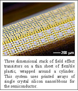
The researchers report several demonstration systems that involve wide ranging types of devices, including silicon MOSFETs, GaN HEMTs, GaAs diodes and even transistors that use carbon nanotubes, formed in various combinations on rigid as well as mechanically flexible substrates in single and multilayer configurations. The figure shows an optical image of a three layer stack of high performance transistors that incorporate printed single crystal silicon nanoribbons. This system uses a thin, flexible sheet of plastic as a substrate. The image shows the circuit bent around a cylindrical support to illustrate its mechanical flexibility.
Besides these examples, the researchers believe that the same methods will enable integration of optical, sensing and micromechanical devices with these electronics to yield complete, multifunctional systems.

J.-H. Ahn, H.-S. Kim, K.J. Lee, S. Jeon, S.J. Kang, Y. Sun, R.G. Nuzzo and J.A. Rogers, Science 314, 1754. 15 December 2006


