Semiconductor Polishing: New Spherical Nanoparticle Abrasive Could Advance Chemical-Mechanical Planarization in Integrated Circuit Production
14 Jun, 2006 01:11 pm
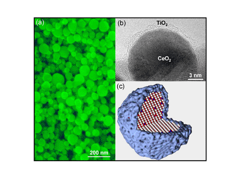
Semiconductor polishing ? known technically as chemical-mechanical planarization (CMP) ? has become more critical as feature sizes on integrated circuits (ICs) have become smaller. Surfaces must now be flat to within sub-nanometer tolerances and free of defects. And next-generation devices will have to meet even tougher standards. Nanoparticles made of cerium oxide (CeO2) ? also known as ceria ? are now used to polish semiconductor wafers between the more than two-dozen processing steps needed to make a modern integrated circuit. But because of irregular crystalline shapes in the existing material, that polishing can scratch wafer surfaces and significantly reduce the yield of IC devices. To address that problem, a research team led by Dr. Xiangdong Feng from Ferro and Prof. Zhong Lin Wang from Georgia Tech took advantage of differential melting temperatures between two oxide materials to create a new type of spherical cerium oxide nanoparticles that roll like a ball bearing [1].

Figure: (a) Scanning electron microscopy image of single crystal nanospheres of Ti dopped CeO2 nanoparticles. (b) Transmission electron microscopy image of a single crystal CeO2 nanosphere enclosed by a thin shell of amorphous TiO2. (c) Molecular dynamic simulated structure of Ti dopped CeO2 nanosphere.
[1] Science 312 (2006) 1504


